$764.86 Million Atomic Force Microscopy Market Booms in 2025: Japan, Germany, and U.S. Advance Nanotechnology Research
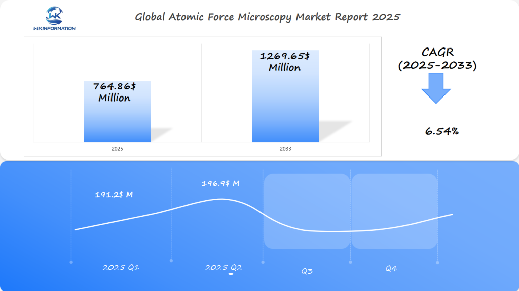
In 2025, the global Atomic Force Microscopy Market reached an estimated value of USD 764.86 Million, with projections indicating growth to USD 1269.65 Million by 2033 at a compound annual growth rate (CAGR) of 6.54%.
- Last Updated:
Atomic Force Microscopy Market Q1 and Q2 2025 Forecast
The Atomic Force Microscopy (AFM) market is projected to reach $764.86 million in 2025, with a CAGR of 6.54% from 2025 to 2033. In Q1 2025, the market is expected to generate approximately $191.2 million, with significant demand from Japan, Germany, and the U.S. due to the increasing adoption of AFM in nanotechnology, material science, and biological research.
By Q2 2025, the market is forecast to reach $196.9 million, driven by expanding applications in biotechnology, pharmaceutical research, and semiconductor manufacturing. The U.S. and Germany will see strong growth in research applications, particularly in nanoelectronics and advanced materials testing, while Japan remains a key player in the nanotechnology sector.
Understanding the AFM Industry: Key Players and Applications
The Atomic Force Microscopy (AFM) industry chain is a complex world of innovation and parts that work together. At its heart, AFM technology connects suppliers and users in many scientific and industrial areas.
Who are the Upstream Suppliers?
Upstream suppliers are key in the AFM chain. They give important parts:
- Precision probe makers
- Laser and optical system creators
- Advanced material suppliers
- Nanoscale sensing tech makers
These suppliers make complex parts that help AFM devices see and measure tiny things. Their work improves AFM’s ability to show details at the nanoscale, helping nanoscale research grow.
Where is AFM Used?
AFM’s uses are wide, showing its flexibility:
- Semiconductor research and development
- Biological and medical imaging
- Materials science studies
- Nanotechnology product design
Places like research labs, industrial labs, and tech companies use AFM to see tiny details. The detailed AFM industry chain lets scientists see and work with materials at the nanometer scale. This opens new ways to understand science.
AFM technology changes how researchers study and understand tiny worlds in many fields.
Key Trends Driving the Atomic Force Microscopy Market: Demand in Nanotechnology and Materials Science
The atomic force microscopy (AFM) market is growing fast. This is thanks to new uses in nanotechnology and materials science. Researchers and companies are using AFM to study materials at the nanoscale with great detail.
Key trends shaping the AFM market include:
- Expanding nanotechnology applications in semiconductor manufacturing
- Advanced materials development and characterization
- Cutting-edge research in life sciences and biomedical engineering
AFM’s Role in Advancing Materials Science Research
Scientific teams are using AFM to advance materials science research. Nanoscale imaging capabilities are key for studying material properties and interactions. This is important across many fields.
“Atomic force microscopy represents a quantum leap in our ability to visualize and manipulate matter at the molecular level.” – Dr. Elizabeth Chen, Nanotechnology Research Institute
Benefits of AFM in the Semiconductor Industry
The semiconductor industry is also benefiting from AFM. It uses high-resolution imaging for quality checks and new product ideas. Researchers can see surface details, measure material strength, and check what materials are made of with high accuracy.
New uses for AFM are leading to more investment and innovation. This makes the market look set to grow even more in the future.
Challenges in Atomic Force Microscopy Development and Cost Barriers
Atomic Force Microscopy (AFM) is a key tool in nanotechnology research. But, it faces big challenges that slow its use. The main issues are complex technology and high costs needed to use this advanced tool.
The biggest cost hurdles in AFM development are:
- High initial equipment costs
- Need for special training for researchers
- Expensive maintenance and calibration
- Complex setup needed
Technological limitations also block progress. AFM systems need precise engineering and advanced software. This raises costs. Researchers face technical hurdles like:
- Getting high nanoscale resolution
- Reducing environmental impact
- Creating more sensitive scans
- Lowering measurement errors
“The future of AFM relies on overcoming current technological constraints through innovative research and strategic investments.” – Nanotechnology Research Institute
Research groups and tech companies are working to solve these problems. They aim to make AFM systems cheaper, easier to use, and more affordable. New solutions aim to simplify things, make automation better, and cut down on costs.

Geopolitical Influence on the Atomic Force Microscopy Market
The global atomic force microscopy (AFM) market is deeply tied to complex geopolitical landscapes. International research collaboration and trade policies are key in shaping technological progress and market trends across regions.
Investments in nanotechnology have become a strategic focus for global scientific communities. North America leads the AFM market, thanks to its strong research infrastructure and technological prowess.
- United States leads in advanced research investments
- European nations demonstrate strong collaborative frameworks
- Asian Pacific markets exhibit rapid technological growth
The AFM market geopolitics show complex patterns of technological exchange and strategic partnerships. Countries like China, Japan, and India are quickly growing their nanotechnology research, challenging the traditional leaders.
Trade policies and technology transfer restrictions greatly affect the AFM market. International research collaboration is vital for navigating these complex geopolitical landscapes. It enables knowledge sharing and technological innovation across borders.
Atomic Force Microscopy Market by Type: Contact Mode, Non-Contact Mode, and Tapping Mode
Atomic Force Microscopy (AFM) lets researchers study tiny details. It has different modes for looking at surfaces and materials at the molecular level.
The three main AFM types are different ways to scan and study surfaces:
- Contact mode AFM
- Non-contact mode AFM
- Tapping mode AFM
Contact Mode AFM
Contact mode AFM touches the sample surface. It’s used for hard, stable materials that can be scanned directly.
- Provides high-resolution topographical data
- Best suited for hard, uniform surfaces
- Enables precise surface measurement
Non-Contact Mode AFM
Non-contact mode AFM keeps a small distance from the sample. It’s safe for delicate or fragile specimens.
- Ideal for soft biological samples
- Reduces risk of surface modification
- Excellent for measuring electrostatic forces
Tapping Mode AFM
Tapping mode AFM moves the probe in a way that touches the surface briefly. It balances detail with gentle interaction.
- Provides superior surface detail
- Minimizes lateral forces
- Suitable for multiple material types
Each AFM type has its own benefits. Researchers can choose the best mode for their study.
Applications of Atomic Force Microscopy in Semiconductor, Biophysics, and Surface Analysis
Atomic Force Microscopy (AFM) has changed the game in science. It gives us deep insights into materials and living things. It’s used in many areas, like the semiconductor field, biophysics, and studying surfaces.
Applications of AFM in Semiconductor
In the semiconductor world, AFM is key for checking out tiny electronic parts. Scientists use it to:
- Look at the surface of microchips
- Study the properties of semiconductor materials
- Check how nanoscale devices are made
- Find tiny flaws in electronics
Applications of AFM in Biophysics
Biophysics uses AFM to see how molecules interact closely. Scientists can now see:
- The shape of cell membranes
- How proteins fold
- The shape of DNA and RNA
- How molecules interact at the nanoscale
Applications of AFM in Surface Analysis
Surface analysis is another area where AFM shines. It lets researchers study material details with incredible precision. They can learn about surface properties, roughness, and what’s on the surface.
AFM is a game-changing tool. It connects seeing tiny things with deep scientific knowledge in many fields.
Global Insights into the Atomic Force Microscopy Market
The global AFM market is a key area for new technology and research. It has grown a lot in recent years. Experts say it will keep growing in many places.
Here are some important points about the global AFM market:
- Market valuation reached $764.86 million in 2025
- Projected growth to $1269.65 million by 2033
- Strong research investments driving market development
Different regions have different levels of technology. North America and Europe are leaders in research. Asia-Pacific is catching up fast.
“The atomic force microscopy market represents a critical frontier in scientific research and technological innovation.” – Dr. Katherine Roberts, Nanotechnology Research Institute
Experts predict the market will keep growing. This is because of new technology, more funding for research, and more uses in fields like semiconductors and biophysics.
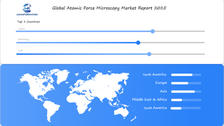
Japan's Leadership in High-Precision Nanotechnology and AFM Equipment
Japan leads the world in the AFM market, making big strides in nanotechnology. Its tech skills make it a key player in making advanced microscopy tools. Japanese AFM makers are known for their top-notch precision and engineering.
The country is all in on nanotechnology research in many areas:
- Advanced semiconductor research
- Materials science innovations
- Biomedical technology development
- High-resolution imaging techniques
Big Japanese companies are world leaders in atomic force microscopy. Their tools let scientists see tiny things with great detail. Cutting-edge places like RIKEN and University of Tokyo keep improving how we see the tiny world.
| Japanese AFM Manufacturer | Key Specialization | Global Market Impact |
|---|---|---|
| Shimadzu Corporation | Precision Instrumentation | High-Performance Imaging Systems |
| JEOL Ltd. | Electron Microscopy | Advanced Nanotechnology Solutions |
| Hitachi High-Technologies | Research Equipment | Comprehensive Scientific Instruments |
Government support and research partnerships have helped Japan’s nanotech scene grow. By working together, schools and companies keep Japan ahead in science.
Germany's Advancements in Materials Science and Industrial Microscopy
Germany leads in materials science research, driving big innovations in the Germany AFM market. Its precision engineering makes it a global leader in industrial microscopy. This pushes the limits of nanotechnology and advanced scientific study.
The country’s research centers have made big strides in atomic force microscopy, focusing on several key areas:
- Advanced probe design for high-resolution imaging
- Sophisticated software algorithms for data analysis
- Integrated microscopy systems with enhanced precision
German researchers collaborate with top international scientific groups to explore new materials science applications. Their work covers fields like semiconductor research, biophysics, and nanomaterial characterization.
| Research Focus | Key Contributions |
|---|---|
| Nanotechnology | Precision imaging techniques |
| Materials Engineering | Advanced surface analysis methods |
| Industrial Microscopy | High-resolution scanning technologies |
The industrial microscopy landscape in Germany keeps growing, with big investments in research and development. Universities and private research centers are always pushing the tech limits, creating new solutions for complex scientific problems.
These steps show Germany’s dedication to staying ahead in materials science research and tech innovation. This solidifies its role in the global AFM market. Additionally, recent studies have also highlighted the importance of data-driven approaches in enhancing the efficiency and accuracy of these advancements.
The U.S.'s Expanding Research in Life Sciences and Advanced Imaging Technologies
The United States is leading in advanced imaging technology research, especially in the US AFM market. Top labs and research centers are pushing the limits of life sciences with atomic force microscopy (AFM).
Research centers are making big strides in understanding tiny biological systems. Universities and national labs use advanced imaging to study molecules, cells, and complex biological processes.
“Atomic force microscopy represents a transformative tool in modern scientific research, enabling unprecedented visualization of nanoscopic environments,” says Dr. Elizabeth Roberts, leading nanotechnology researcher.
Key Drivers of Research Advancement
Several factors contribute to the advancement of research in life sciences and advanced imaging technologies:
- National Institutes of Health (NIH) funding significant AFM research projects
- Interdisciplinary collaborations between biology, physics, and engineering departments
- Development of high-resolution imaging techniques for medical diagnostics
The US AFM market is growing with investments in nanotechnology and life sciences. Researchers are creating advanced imaging tools that expand our scientific knowledge.
| Research Focus | Key Institutions | Primary Applications |
|---|---|---|
| Nanomedicine | Stanford University | Drug delivery mechanisms |
| Cellular Imaging | Harvard Medical School | Cancer research |
| Materials Characterization | MIT Nanotechnology Lab | Advanced material design |
New technologies are changing science, with the U.S. at the forefront. They are developing advanced AFM methods for major breakthroughs in life sciences.
The Future of Atomic Force Microscopy: AI-Powered Analysis and High-Resolution Enhancements
The world of atomic force microscopy (AFM) is changing fast. New AI tools and high-resolution imaging are making big changes in science. These advancements are opening up new ways for scientists to study tiny things.
Some big changes in AFM are making science better:
- Artificial intelligence integration for automated data processing
- Enhanced real-time image analysis techniques
- Unprecedented high-resolution imaging capabilities
- Automated sample preparation methodologies
Companies like Park Systems and Bruker are leading the way. They’re making AFM systems that use AI. These systems can show tiny details with great accuracy, helping scientists see the world in new ways.
High-resolution imaging is getting even better thanks to AI. These smart tools can quickly understand complex data. This means scientists can make new discoveries faster in fields like materials science and biotechnology.
The convergence of artificial intelligence and atomic force microscopy represents a transformative moment in scientific instrumentation.
Places like universities and tech companies are putting a lot of money into AFM. They want to make systems that can show real-time, dynamic visualization of tiny things. These new tools will help us learn more about the tiny world around us.
Competitive Landscape in the Atomic Force Microscopy Market
The atomic force microscopy (AFM) market is very competitive. Global manufacturers are always coming up with new ideas. They aim to get a big share of the market and push the boundaries of nanotechnology research.
Some big names in the AFM market include:
- Bruker Corporation —— United States
- Park Systems —— South Korea
- Oxford Instruments —— United Kingdom
- Hitachi High-Tech Corporation —— Japan
- Horiba Ltd. —— Japan
- Nanosurf AG —— Switzerland
- WITec GmbH —— Germany
- NT-MDT Spectrum Instruments —— Russia
- NanoMagnetics Instruments —— Turkey
- Nanonics Imaging —— Israel
Overall
|
Report Metric |
Details |
|---|---|
| Report Name | Global Atomic Force Microscopy Market Report |
| Base Year | 2024 |
| Segment by Type |
|
| Segment by Application |
|
| Geographies Covered |
|
| Forecast units | USD million in value |
| Report coverage | Revenue and volume forecast, company share, competitive landscape, growth factors and trends |
Atomic Force Microscopy (AFM) has changed the game in science and industry. It gives us a close look at tiny materials. Bruker Corporation leads in making these advanced tools.
AFM has changed how we make semiconductors, study materials, and work in biotech. It lets us see and move single atoms. This has led to new discoveries in electronics, medicine, and materials.
AFM’s effects go beyond the lab. It’s helping make better medical tools, energy tech, and gadgets. It’s changing how we see the world, one tiny step at a time.
As we keep learning, AFM gets even better. It gives us more detailed views of materials. This means we’re on the path to solving big problems with tiny tools.
Global Atomic Force Microscopy Market Report (Can Read by Free sample) – Table of Contents
Chapter 1: Atomic Force Microscopy Market Analysis Overview
- Competitive Forces Analysis (Porter’s Five Forces)
- Strategic Growth Assessment (Ansoff Matrix)
- Industry Value Chain Insights
- Regional Trends and Key Market Drivers
- Atomic Force MicroscopyMarket Segmentation Overview
Chapter 2: Competitive Landscape
- Global Atomic Force Microscopyplayers and Regional Insights
- Key Players and Market Share Analysis
- Sales Trends of Leading Companies
- Year-on-Year Performance Insights
- Competitive Strategies and Market Positioning
- Key Differentiators and Strategic Moves
Chapter 3: Atomic Force Microscopy Market Segmentation Analysis
- Key Data and Visual Insights
- Trends, Growth Rates, and Drivers
- Segment Dynamics and Insights
- Detailed Market Analysis by Segment
Chapter 4: Regional Market Performance
- Consumer Trends by Region
- Historical Data and Growth Forecasts
- Regional Growth Factors
- Economic, Demographic, and Technological Impacts
- Challenges and Opportunities in Key Regions
- Regional Trends and Market Shifts
- Key Cities and High-Demand Areas
Chapter 5: Atomic Force Microscopy Emerging and Untapped Markets
- Growth Potential in Secondary Regions
- Trends, Challenges, and Opportunities
Chapter 6: Product and Application Segmentation
- Product Types and Innovation Trends
- Application-Based Market Insights
Chapter 7: Atomic Force Microscopy Consumer Insights
- Demographics and Buying Behaviors
- Target Audience Profiles
Chapter 8: Key Findings and Recommendations
- Summary ofAtomic Force Microscopy Market Insights
- Actionable Recommendations for Stakeholders
Access the study in MULTIPLEFORMATS
Didn’t find what you’re looking for?
TALK TO OUR ANALYST TEAM
Need something within your budget?
NO WORRIES! WE GOT YOU COVERED!
Call us on: +1-866-739-3133
Email: infor@wkinformation.com
What is Atomic Force Microscopy (AFM)?
Atomic Force Microscopy is a tool that lets us see and study tiny things. It shows us the surface details of materials at a very small scale. This helps in many fields, from science to industry.
How does AFM contribute to nanotechnology research?
AFM helps scientists see and work with tiny structures. It gives us important information about materials and how they interact. This is key for improving materials and understanding how they work.
What are the primary modes of Atomic Force Microscopy?
AFM works in three main ways:
- Contact mode: The probe touches the surface being scanned.
- Non-contact mode: The probe hovers above the surface without making contact.
- Tapping mode: The probe vibrates near the surface, making intermittent contact.
Each method is best suited for different types of materials and applications.
What is the projected market value for Atomic Force Microscopy?
The market for AFM is expected to grow to $764.86 million by 2025. This growth is due to new technologies and more research in fields like nanotechnology and life sciences.
Which countries are leading in AFM technology development?
Japan, Germany, and the United States are leading in AFM. They have unique strengths in making precise products, studying materials, and creating advanced images.
What challenges exist in AFM technology?
Challenges include high costs, needing special training, and complex use. But, scientists are working to make AFM easier and more accessible.
Which industries benefit the most from Atomic Force Microscopy?
Atomic Force Microscopy (AFM) is used in various industries, including:
- Semiconductors
- Biophysics
- Materials science
- Healthcare
AFM plays a crucial role in these fields by providing insights into surface details and molecular interactions.
How is artificial intelligence impacting AFM technology?
AI is changing AFM by analyzing data, preparing samples, and processing images in real-time. It’s making research more advanced and efficient.
What makes AFM unique compared to other microscopy techniques?
AFM has several features that set it apart from other microscopy techniques:
- Versatility: AFM can be used on a wide range of materials, including metals, polymers, and biological samples.
- 3D Imaging: Unlike some other techniques that only provide 2D images, AFM produces detailed three-dimensional representations of the sample’s surface.
- Operating Conditions: AFM can operate in various environments, including air, vacuum, and liquid conditions. This makes it suitable for studying samples in their natural state or under specific conditions.
- Atomic Manipulation: One of the most remarkable capabilities of AFM is its ability to manipulate individual atoms or molecules. This opens up possibilities for precise engineering at the nanoscale.
These unique features make AFM a powerful tool for researchers in fields such as materials science, nanotechnology, and biology.
What is the future outlook for Atomic Force Microscopy?
AFM’s future looks bright with ongoing improvements and new uses. It will likely be used more in fields like nanomedicine and quantum computing.source
RECENT REPORTS
Our clients