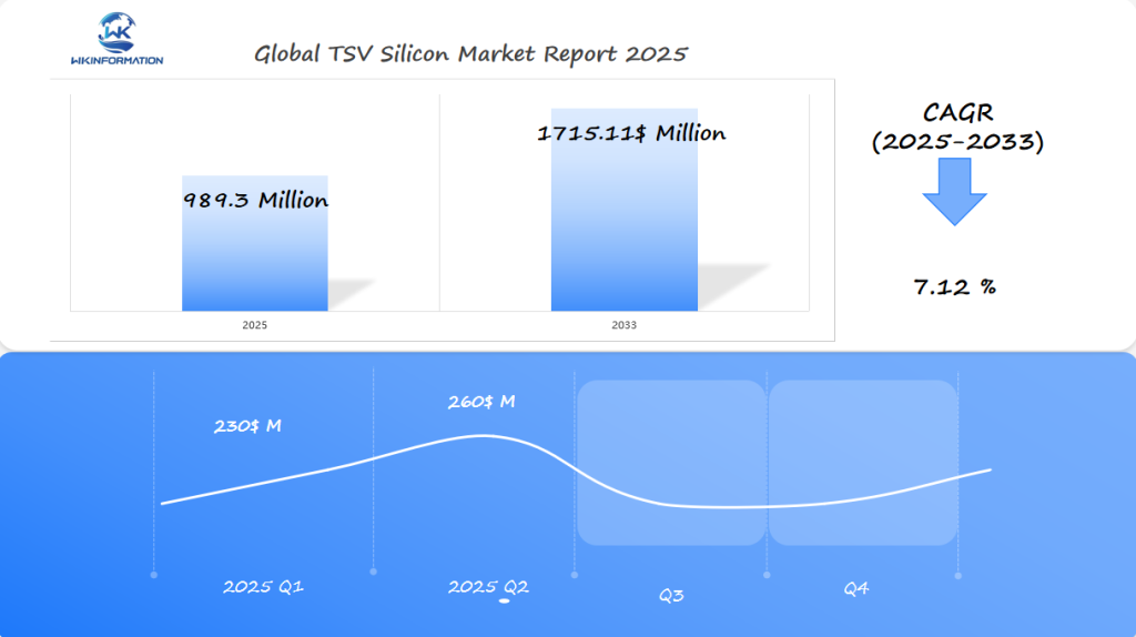
TSV Silicon Market Forecast to Reach $989.3 Million Globally by 2025: Semiconductor Packaging Advances in Taiwan, South Korea, and U.S.
Explore the TSV Silicon Market growth driven by 3D integration, advanced semiconductor packaging, and IoT applications. Analysis shows robust expansion with key industry players leading innovation.
- Last Updated:
TSV Silicon Market Analysis and Forecast for Q1 and Q2 2025
The TSV Silicon market is projected to reach $989.3 million in 2025, supported by a robust CAGR of 7.12% over the 2025-2033 period. The market is estimated to record about $230 million in Q1 2025 and expand to approximately $260 million in Q2, reflecting increasing demand in advanced semiconductor packaging and 3D integration technologies. The continual push toward miniaturization and enhanced chip performance is driving adoption of TSV Silicon in key electronics sectors including mobile devices and data centers.
Key Takeaways
- TSV silicon market expected to reach $989.3 million by 2025
- Technology enables advanced 3D IC integration
- Supports increasing demand for compact electronic devices
- Critical for next-generation semiconductor packaging
Upstream and downstream industry chain insights for TSV silicon technology
The semiconductor supply chain for Through-Silicon Via (TSV) technology is complex. It involves many players working together to innovate in advanced packaging. This network goes from raw material suppliers to top-notch semiconductor foundries, building a strong base for the latest electronic parts.
Upstream: Key players in the TSV silicon technology supply chain
- Raw material procurement: Silicon wafer manufacturers rely on a steady supply of high-quality raw materials, such as silicon crystals and other semiconductor materials, to produce wafers used in TSV technology.
- Advanced equipment development: Precision manufacturing processes are critical for achieving the required accuracy in TSV fabrication. Companies involved in developing advanced equipment, such as lithography machines and etching tools, play a vital role in ensuring the success of TSV production.
- Semiconductor foundry processing: Foundries are responsible for fabricating semiconductor devices using TSV technology. They leverage their expertise in advanced manufacturing techniques to integrate multiple chips vertically and enhance overall performance.
Downstream: Services that support the implementation of TSV silicon technology
- Packaging and integration services: After the fabrication process, packaging and integration services come into play. These services involve encapsulating the semiconductor devices with TSVs and integrating them into larger systems or modules.
- Testing and validation: To ensure the reliability and functionality of TSV-enabled products, rigorous testing and validation processes are conducted. This includes electrical testing, thermal analysis, and mechanical assessments to verify performance under various conditions.
Raw Material Suppliers and Equipment Manufacturers
Silicon wafer makers are key in starting TSV technology. Companies like Shin-Etsu and Siltronic create precise substrates needed for advanced semiconductor packaging.
Semiconductor Foundries and Packaging Houses
Semiconductor foundries like TSMC and Samsung push TSV technology forward. They turn raw materials into complex integrated circuits with advanced packaging. This leads to better performance and smaller sizes.
Working together, equipment makers, silicon wafer producers, and semiconductor foundries drive TSV technology’s growth in the global market.
Market trends in 3D IC packaging and miniaturization
The semiconductor industry is changing fast. It’s all about making devices smaller and more advanced. 3D IC packaging is key to creating compact, high-performance electronics.
Electronic design is evolving quickly. Manufacturers are exploring new limits in semiconductor technology. They’re making devices that are more powerful, efficient, and take up less space and energy.
Increasing Demand for Compact Electronic Devices
People want smaller, more powerful electronics. This is changing how we package semiconductors. Key trends include:
- Reduction in device size by up to 70%
- Enhanced performance through vertical chip stacking
- Improved heat management in compact designs
Advancements in Heterogeneous Integration
Heterogeneous integration is a big step in 3D IC packaging. It lets manufacturers mix different semiconductor technologies in one package. This leads to:
- Enhanced system-level performance
- More efficient use of silicon real estate
- Reduced interconnect complexity
Thanks to through-silicon via (TSV) technology, we can now make ultra-compact devices. They offer unmatched computational power and energy efficiency.
Regulatory restrictions related to semiconductor manufacturing
The semiconductor industry faces a complex landscape of regulations. These rules significantly impact manufacturing processes and global market dynamics. As technology advances, environmental and trade policies become more important.
Semiconductor manufacturers must navigate a challenging regulatory environment. This environment includes multiple critical areas:
- Environmental compliance requirements
- Export control restrictions
- Chemical usage and waste management protocols
- International trade policy constraints
Environmental Regulations and Compliance
Environmental compliance is now a top concern for semiconductor production facilities. Manufacturers must implement rigorous waste management strategies and reduce chemical emissions. The industry is focusing on sustainable manufacturing processes to minimize environmental impact.
| Regulatory Area | Key Requirements | Compliance Impact |
| Chemical Management | Reduced hazardous substance usage | Increased production costs |
| Waste Disposal | Strict recycling and treatment protocols | Enhanced environmental protection |
| Emissions Control | Lower carbon footprint standards | Technological innovation |
Export Controls and Trade Policies
Export controls have become a critical factor in the semiconductor supply chain. Governments are implementing strict trade policies to protect national technological interests. Semiconductor regulations now play a crucial role in managing international technology transfers.
The semiconductor industry must continuously adapt to evolving regulatory landscapes. It must balance technological innovation with compliance requirements. Strategic planning and a proactive approach to regulatory challenges will be key to maintaining competitive advantage in the global market.

Geopolitical impacts on supply chain and production facilities
The semiconductor industry is now a key area of global competition. Geopolitical tensions have changed the supply chain, causing big challenges for makers and tech companies everywhere.
International trade has made semiconductor production hard. Several important factors have come up:
- Escalating US-China trade restrictions
- Increasing national security concerns
- Strategic realignment of global manufacturing capabilities
US-China Trade Tensions and Their Effects
The trade fights between the US and China have made things tough for the global semiconductor supply chain. Export controls and tech transfer limits have made companies change their plans for making and getting parts.
Global Chip Shortage and Mitigation Strategies
The chip shortage has revealed the vulnerabilities in the semiconductor supply chain. Companies are exploring various strategies to reduce risks and maintain steady production:
- Diversifying manufacturing locations
- Investing in domestic production capabilities
- Developing more resilient supply chain networks
Semiconductor manufacturers are realizing that maintaining stability is just as crucial as being at the forefront of technology. This is essential for remaining competitive in the market.
Segmentation by silicon wafer type and TSV dimensions
The through-silicon via (TSV) technology is a big step forward in semiconductor packaging. It allows for smaller and more powerful devices. The type of silicon wafer and the size of the TSVs are key to how well 3D integrated circuits work.
Companies are trying different ways to use TSV technology. Each method has its own strengths and uses.
Via-First, Via-Middle, and Via-Last TSV Approaches
There are three main ways to use TSV technology:
- Via-first TSV: Vias are made before the devices are built. This method is very precise.
- Via-middle TSV: Vias are made during the device building process.
- Via-last TSV: Vias are made after the devices are built. This gives the most design freedom.
Micro-TSV and Macro-TSV Applications
The size of the TSVs affects how well semiconductors work and how they can be used:
| TSV Type | Diameter Range | Primary Applications |
| Micro-TSV | 1-10 μm | High-density memory, mobile devices |
| Macro-TSV | 50-100 μm | Power devices, sensor integration |
The semiconductor industry is always looking to improve TSV technology. They are working on new ways to make devices smaller and more powerful.
Application analysis across memory, logic, and sensor devices
Through-silicon via (TSV) technology has changed how semiconductors are made. It has led to big steps forward in memory devices, logic ICs, and sensors. These new uses of TSV are making electronics smaller and more efficient in many fields.
DRAM and NAND Flash Memory Innovations
TSV technology has made memory devices much better. In DRAM and NAND flash memory, TSVs help pack more data into smaller spaces. This means we can store more information without needing bigger devices.
- Enhanced vertical stacking capabilities
- Improved electrical signal transmission
- Reduced power consumption
Logic IC Performance Enhancements
Logic ICs, like processors and FPGAs, get a big boost from TSVs. This tech lets them handle more complex tasks. It also makes them faster and more efficient.
| Logic IC Type | TSV Benefits | Performance Improvement |
| Microprocessors | Compact 3D integration | 15-25% speed increase |
| FPGAs | Enhanced signal routing | 10-20% power efficiency |
MEMS and Image Sensor Integration
MEMS sensors also benefit a lot from TSVs. This tech helps make sensors better at picking up signals and less prone to interference. Image sensors see huge improvements thanks to TSVs.
TSV technology keeps getting better. It’s making semiconductors smaller and more powerful. This is changing many areas of technology.
Regional perspectives in the global TSV silicon market
The global TSV silicon market shows big differences in different parts of the world. Each area brings its own special strengths to making semiconductors better. Knowing about these areas helps us understand how TSV technology is changing.
Different continents have their own ways of making semiconductors. This shows how technology and making plans vary.
North America’s Technological Leadership
North American companies are leading the way in new TSV technology. They are ahead in research and development. Their main strengths are:
- Advanced research at top universities
- Large investments from venture capitalists
- Strong development of intellectual property
Asia-Pacific’s Manufacturing Dominance
The Asia-Pacific region is a major player in producing TSV silicon. Countries such as Taiwan and South Korea are crucial in this industry.
Key Factors Behind Asia-Pacific’s Success
Several factors contribute to the success of the Asia-Pacific region in manufacturing TSV silicon:
- High-volume production capabilities: The ability to produce large quantities of silicon wafers efficiently.
- Advanced semiconductor fabrication facilities: State-of-the-art manufacturing plants equipped with cutting-edge technology.
- Substantial government support for technology development: Investments and initiatives from governments to promote research and innovation in the semiconductor sector.
Europe’s Strategic Applications
European areas focus on specific uses of TSV, like in cars and industry. They focus on making things precise and solving unique tech problems.
- Focus on automotive electronics
- Industrial sensor technology innovations
- Sustainable semiconductor manufacturing practices
These views show how the global TSV silicon market is complex and connected. They show how different places help advance technology together.
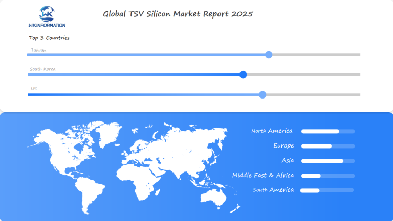
Taiwan's Leadership in Semiconductor Packaging
The Taiwan semiconductor industry is at the top of global tech innovation. TSMC leads in advanced packaging technologies. Taiwan has a strong ecosystem for cutting-edge research and manufacturing.
TSMC has changed the game with Through-Silicon Via (TSV) technology. They’ve created new packaging methods for smaller, more efficient chips. Semiconductor packaging innovations show Taiwan’s tech strength.
Strategic Collaborations in Semiconductor Manufacturing
TSMC and OSAT companies work together to push tech limits. Their partnership creates a special place for innovation in the semiconductor world:
- Advanced packaging integration
- Shared research and development initiatives
- Enhanced manufacturing efficiency
- Rapid prototype development
Driving Global Semiconductor Innovation
Taiwanese manufacturers are global leaders in high-precision manufacturing and technological advancement. Foundries and OSAT companies collaborate closely to drive rapid technological progress. This synergy positions Taiwan as a crucial player in the global semiconductor industry.
South Korea's advanced memory and logic chip production
The South Korean semiconductor industry is a global leader in technology. Samsung Electronics and SK Hynix are at the forefront. They have changed the game in memory and logic chip making with smart investments and research.
South Korea does more than just make chips. It has a strong system that helps keep technology moving forward. This is especially true for through-silicon via (TSV) technologies.
Samsung and SK Hynix’s TSV Implementations
Samsung Electronics and SK Hynix have been key in creating advanced TSV technologies. These technologies help make:
- Higher memory density
- Improved signal performance
- Reduced power consumption
- Compact semiconductor packaging
R&D Investments in Next-Generation TSV Technologies
These companies are all in on innovation. They spend a lot on research and development. SK Hynix and Samsung Electronics are always looking for new ways to improve TSV technologies.
Their research aims to make TSV technologies better. They want to support the growing needs of artificial intelligence and edge computing.
U.S. Innovation in Semiconductor Materials
The United States is leading in semiconductor technology, especially in Through-Silicon Via (TSV) materials. This innovation puts the U.S. at the top for creating new solutions for future electronics.
Top companies are working together to improve TSV materials. They team up with universities to mix research with real-world use. New research is looking into ways to make semiconductors better and more reliable.
Development of Advanced TSV-Compatible Materials
US innovation focuses on several key areas:
- Creating high-conductivity copper-based TSV materials
- Developing low-k dielectric insulators for better signal quality
- Exploring nano-engineered barrier layers
Collaboration Between Academia and Industry
Working together, research places and companies are crucial for TSV advancements. Industry-academia collaboration leads to quick testing and major discoveries. These discoveries help push technology further.
Places like Stanford University and MIT are teaming up with Intel and Nvidia. They aim to create new TSV materials for more complex semiconductors.
Future development prospects for TSV silicon technology
The world of semiconductors is changing fast, with TSV silicon technology leading the way. The global market is growing, and researchers are working on new uses. These new uses could change how we compute forever.
- AI applications needing super-fast computing
- Edge computing that needs to work quickly
- Advanced packaging for new electronic devices
Emerging Applications in AI and Edge Computing
AI and edge computing are driving advancements in TSV tech. Miniaturized semiconductor designs enhance computer performance while reducing energy consumption. This is beneficial for intricate AI operations and rapid data processing across various industries.
Integration with Advanced Packaging Technologies
Advanced packaging is a significant area for TSV silicon technology. Companies are working on new ways to assemble chips, resulting in:
- More transistors in a smaller space
- Improved cooling for chips
- Faster signal transmission
The semiconductor industry is expected to continue growing, with new applications in self-driving cars, medical devices, and smart systems. TSV technology is poised to make future electronics faster and more efficient.
Competitive landscape of key manufacturers
Key players in the Through-Silicon Via (TSV) market are focusing on technological advancements to enhance 3D integrated circuit performance and miniaturization. They are expanding operations in regions such as Asia-Pacific and North America, where demand for high-performance computing, consumer electronics, and automotive applications is increasing.
Key Players:
-
TSMC (Taiwan)
-
Intel Corporation (United States)
-
Samsung Electronics (South Korea)
-
GlobalFoundries (United States)
-
Micron Technology (United States)
-
SK Hynix (South Korea)
-
Tower Semiconductor (Israel)
-
ASE Group (Taiwan)
-
Amkor Technology (United States)
-
STMicroelectronics (Switzerland / France)
Overall
| Report Metric | Details |
|---|---|
| Report Name | Global TSV Silicon Market Report |
| Base Year | 2024 |
| Segment by Type |
· Micro-TSV · Macro-TSV |
| Segment by Application |
· Memory · Logic · Sensor Devices |
| Geographies Covered |
· North America (United States, Canada) · Europe (Germany, France, UK, Italy, Russia) · Asia-Pacific (China, Japan, South Korea, Taiwan) · Southeast Asia (India) · Latin America (Mexico, Brazil) |
| Forecast units | USD million in value |
| Report coverage | Revenue and volume forecast, company share, competitive landscape, growth factors and trends |
Global TSV Silicon Market Report (Can Read by Free sample) – Table of Contents
Chapter 1: TSV Silicon Market Analysis Overview
- Competitive Forces Analysis (Porter’s Five Forces)
- Strategic Growth Assessment (Ansoff Matrix)
- Industry Value Chain Insights
- Regional Trends and Key Market Drivers
- TSV Silicon Market Segmentation Overview
Chapter 2: Competitive Landscape
- Global TSV Silicon Players and Regional Insights
- Key Players and Market Share Analysis
- Sales Trends of Leading Companies
- Year-on-Year Performance Insights
- Competitive Strategies and Market Positioning
- Key Differentiators and Strategic Moves
Chapter 3: TSV Silicon Market Segmentation Analysis
- Key Data and Visual Insights
- Trends, Growth Rates, and Drivers
- Segment Dynamics and Insights
- Detailed Market Analysis by Segment
Chapter 4: Regional Market Performance
- Consumer Trends by Region
- Historical Data and Growth Forecasts
- Regional Growth Factors
- Economic, Demographic, and Technological Impacts
- Challenges and Opportunities in Key Regions
- Regional Trends and Market Shifts
- Key Cities and High-Demand Areas
Chapter 5: TSV Silicon Emerging and Untapped Markets
- Growth Potential in Secondary Regions
- Trends, Challenges, and Opportunities
Chapter 6: Product and Application Segmentation
- Product Types and Innovation Trends
- Application-Based Market Insights
Chapter 7: TSV Silicon Consumer Insights
- Demographics and Buying Behaviors
- TargetAudience Profiles
Chapter 8: Key Findings and Recommendations
- Summary of TSV Silicon Market Insights
- Actionable Recommendations for Stakeholders
Access the study in MULTIPLEFORMATS
Didn’t find what you’re looking for?
TALK TO OUR ANALYST TEAM
Need something within your budget?
NO WORRIES! WE GOT YOU COVERED!
Call us on: +1-866-739-3133
Email: infor@wkinformation.com
What is Through Silicon Via (TSV) technology?
Through Silicon Via (TSV) is an advanced method used to connect electronic components vertically through silicon wafers. This innovative approach allows for smaller and more powerful devices, making it a crucial technology in the quest for greater efficiency in electronic gadgets.
How does TSV technology improve electronic device performance?
TSV technology makes devices smaller and faster. It cuts down on signal delays and boosts electrical performance. This leads to gadgets that are quicker, use less energy, and are more complex.
Which industries benefit the most from TSV technology?
TSV technology is a game-changer for many fields. It’s especially useful in:
- Mobile technology
- Telecommunications
- Automotive industry
- Medical equipment
- Data centers
- Advanced imaging
These areas require devices that are both compact and high-performing.
What are the primary manufacturing approaches for TSV?
There are three main ways to make TSV: via-first, via-middle, and via-last. Each method has its own benefits for different needs in semiconductor packaging.
How do geopolitical tensions impact the TSV silicon market?
Geopolitical tensions, such as those between the U.S. and China, have a significant impact on the semiconductor market. These tensions affect supply chains, technology sharing, and market access, forcing companies to explore alternative methods for manufacturing and sourcing their products.
Which regions lead in TSV silicon technology development?
Taiwan and South Korea are leading the way in TSV tech development in Asia. At the same time, North America, particularly the U.S., is leading the charge in innovation. The U.S. is also heavily involved in research on advanced semiconductor materials.
What are the future prospects for TSV technology?
The future looks bright for TSV. It will likely be used in AI, edge computing, and advanced packaging like chiplets. We can also expect better manufacturing and materials to make devices even better and cheaper.
What challenges exist in TSV technology implementation?
Making TSV devices is complex and expensive. There are also issues with heat, keeping signals clear, and finding materials that work well in 3D chips.
How does TSV technology impact memory device performance?
TSV tech makes memory devices like DRAM and NAND flash better. It allows for stacking, reduces distance between parts, and speeds up data transfer.
What regulatory considerations affect TSV silicon market development?
Rules on making devices, export controls, trade policies, and protecting intellectual property are all important. They affect how semiconductors are made and shared around the world.
RECENT REPORTS
Our clients